
A transistor is a semiconductor device used to amplify or switch electronic signals and electrical power. It is composed of semiconductor material with at least three terminals for connection to an external circuit. A voltage or current applied to one pair of the transistor's terminals changes the current through another pair of terminals. Because the controlled (output) power can be higher than the controlling (input) power, a transistor can amplify a signal. Today, some transistors are packaged individually, but many more are found embedded in integrated circuits.
The transistor is the fundamental building block of modern electronic devices, and is ubiquitous in modern electronic systems. Following its development in 1947 by American physicists John Bardeen, Walter Brattain, and William Shockley, the transistor revolutionized the field of electronics, and paved the way for smaller and cheaper radios, calculators, and computers, among other things. The transistor is on the list of IEEE milestones in electronics, and the inventors were jointly awarded the 1956 Nobel Prize in Physics for their achievement.
.jpg)
Assorted discrete transistors. Packages in order from top to bottom: TO-3, TO-126, TO-92, SOT-23.
Contents
1 History
2 Importance
3 Simplified operation
3.1 Transistor as a switch
3.2 Transistor as an amplifier
4 Comparison with vacuum tubes
4.1 Advantages
4.2 Limitations
5 Types
5.1 Bipolar junction transistor (BJT)
5.2 Field-effect transistor (FET)
5.3 Usage of bipolar and field-effect transistors
5.4 Other transistor types
6 Part numbering standards/specifications
6.1 Japanese Industrial Standard (JIS)
6.2 European Electronic Component Manufacturers Association (EECA)
6.3 Joint Electron Devices Engineering Council (JEDEC)
6.4 Proprietary
6.5 Naming problems
7 Construction
7.1 Semiconductor material
7.2 Packaging
7.2.1 Flexible transistors
History
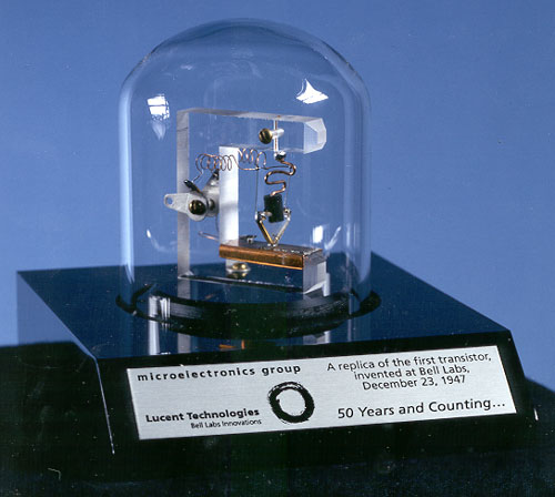
A replica of the first working transistor.
The thermionic triode, a vacuum tube invented in 1907, enabled amplified radio technology and long-distance telephony. The triode, however, was a fragile device that consumed a lot of power. Physicist Julius Edgar Lilienfeld filed a patent for a field-effect transistor (FET) in Canada in 1925, which was intended to be a solid-state replacement for the triode. Lilienfeld also filed identical patents in the United States in 1926 and 1928. However, Lilienfeld did not publish any research articles about his devices nor did his patents cite any specific examples of a working prototype. Because the production of high-quality semiconductor materials was still decades away, Lilienfeld's solid-state amplifier ideas would not have found practical use in the 1920s and 1930s, even if such a device had been built. In 1934, German inventor Oskar Heil patented a similar device.
From November 17, 1947 to December 23, 1947, John Bardeen and Walter Brattain at AT&T's Bell Labs in the United States performed experiments and observed that when two gold point contacts were applied to a crystal of germanium, a signal was produced with the output power greater than the input. Solid State Physics Group leader William Shockley saw the potential in this, and over the next few months worked to greatly expand the knowledge of semiconductors. The term transistor was coined by John R. Pierce as a contraction of the term transresistance. According to Lillian Hoddeson and Vicki Daitch, authors of a biography of John Bardeen, Shockley had proposed that Bell Labs' first patent for a transistor should be based on the field-effect and that he be named as the inventor. Having unearthed Lilienfeld’s patents that went into obscurity years earlier, lawyers at Bell Labs advised against Shockley's proposal because the idea of a field-effect transistor that used an electric field as a "grid" was not new. Instead, what Bardeen, Brattain, and Shockley invented in 1947 was the first point-contact transistor. In acknowledgement of this accomplishment, Shockley, Bardeen, and Brattain were jointly awarded the 1956 Nobel Prize in Physics "for their researches on semiconductors and their discovery of the transistor effect."
In 1948, the point-contact transistor was independently invented by German physicists Herbert Mataré and Heinrich Welker while working at the Compagnie des Freins et Signaux, a Westinghouse subsidiary located in Paris. Mataré had previous experience in developing crystal rectifiers from silicon and germanium in the German radar effort during World War II. Using this knowledge, he began researching the phenomenon of "interference" in 1947. By June 1948, witnessing currents flowing through point-contacts, Mataré produced consistent results using samples of germanium produced by Welker, similar to what Bardeen and Brattain had accomplished earlier in December 1947. Realizing that Bell Labs' scientists had already invented the transistor before them, the company rushed to get its "transistron" into production for amplified use in France's telephone network.
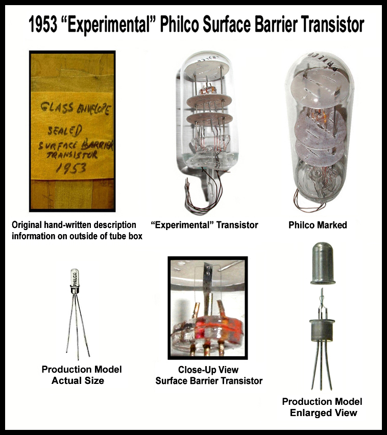
Philco surface-barrier transistor developed and produced in 1953
The first high-frequency transistor was the surface-barrier germanium transistor developed by Philco in 1953, capable of operating up to 60 MHz. These were made by etching depressions into an N-type germanium base from both sides with jets of Indium(III) sulfate until it was a few ten-thousandths of an inch thick. Indium electroplated into the depressions formed the collector and emitter. The first all-transistor car radio, which was produced in 1955 by Chrysler and Philco, used these transistors in its circuitry and also they were the first suitable for high-speed computers.
The first working silicon transistor was developed at Bell Labs on January 26, 1954 by Morris Tanenbaum. The first commercial silicon transistor was produced by Texas Instruments in 1954. This was the work of Gordon Teal, an expert in growing crystals of high purity, who had previously worked at Bell Labs. The first MOS transistor actually built was by Kahng and Atalla at Bell Labs in 1960.
Importance
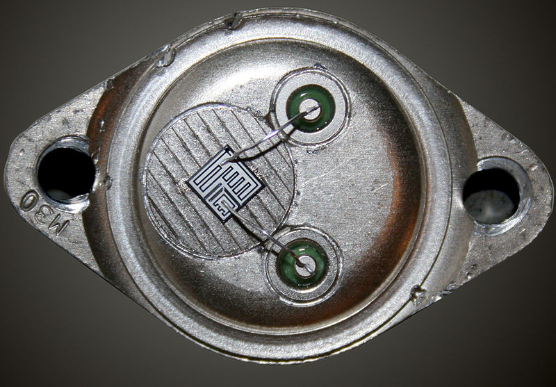
A Darlington transistor opened up so the actual transistor chip (the small square) can be seen inside. A Darlington transistor is effectively two transistors on the same chip. One transistor is much larger than the other, but both are large in comparison to transistors in large-scale integration because this particular example is intended for power applications.
The transistor is the key active component in practically all modern electronics. Many consider it to be one of the greatest inventions of the 20th century. Its importance in today's society rests on its ability to be mass-produced using a highly automated process (semiconductor device fabrication) that achieves astonishingly low per-transistor costs. The invention of the first transistor at Bell Labs was named an IEEE Milestone in 2009.
Although several companies each produce over a billion individually packaged (known as discrete) transistors every year, the vast majority of transistors are now produced in integrated circuits (often shortened to IC, microchips or simply chips), along with diodes, resistors, capacitors and other electronic components, to produce complete electronic circuits. A logic gate consists of up to about twenty transistors whereas an advanced microprocessor, as of 2009, can use as many as 3 billion transistors (MOSFETs). "About 60 million transistors were built in 2002… for [each] man, woman, and child on Earth."
The transistor's low cost, flexibility, and reliability have made it a ubiquitous device. Transistorized mechatronic circuits have replaced electromechanical devices in controlling appliances and machinery. It is often easier and cheaper to use a standard microcontroller and write a computer program to carry out a control function than to design an equivalent mechanical control function.
Simplified operation
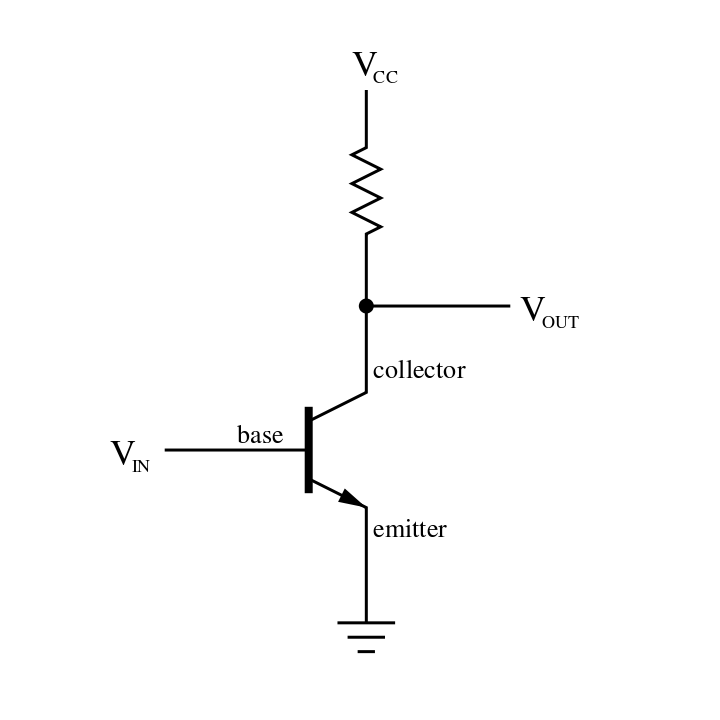
A simple circuit diagram to show the labels of a n–p–n bipolar transistor.
The essential usefulness of a transistor comes from its ability to use a small signal applied between one pair of its terminals to control a much larger signal at another pair of terminals. This property is called gain. It can produce a stronger output signal, a voltage or current, which is proportional to a weaker input signal; that is, it can act as an amplifier. Alternatively, the transistor can be used to turn current on or off in a circuit as an electrically controlled switch, where the amount of current is determined by other circuit elements.
There are two types of transistors, which have slight differences in how they are used in a circuit. A bipolar transistor has terminals labeled base, collector, and emitter. A small current at the base terminal (that is, flowing between the base and the emitter) can control or switch a much larger current between the collector and emitter terminals. For a field-effect transistor, the terminals are labeled gate, source, and drain, and a voltage at the gate can control a current between source and drain.
The image to the right represents a typical bipolar transistor in a circuit. Charge will flow between emitter and collector terminals depending on the current in the base. Because internally the base and emitter connections behave like a semiconductor diode, a voltage drop develops between base and emitter while the base current exists. The amount of this voltage depends on the material the transistor is made from, and is referred to as VBE.
Transistor as a switch
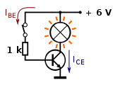
BJT used as an electronic switch, in grounded-emitter configuration.
Transistors are commonly used in digital circuits as electronic switches which can be either in an "on" or "off" state, both for high-power applications such as switched-mode power supplies and for low-power applications such as logic gates. Important parameters for this application include the current switched, the voltage handled, and the switching speed, characterised by the rise and fall times.
In a grounded-emitter transistor circuit, such as the light-switch circuit shown, as the base voltage rises, the emitter and collector currents rise exponentially. The collector voltage drops because of reduced resistance from collector to emitter. If the voltage difference between the collector and emitter were zero (or near zero), the collector current would be limited only by the load resistance (light bulb) and the supply voltage. This is called saturation because current is flowing from collector to emitter freely. When saturated, the switch is said to be on.
Providing sufficient base drive current is a key problem in the use of bipolar transistors as switches. The transistor provides current gain, allowing a relatively large current in the collector to be switched by a much smaller current into the base terminal. The ratio of these currents varies depending on the type of transistor, and even for a particular type, varies depending on the collector current. In the example light-switch circuit shown, the resistor is chosen to provide enough base current to ensure the transistor will be saturated.
In a switching circuit, the idea is to simulate, as near as possible, the ideal switch having the properties of open circuit when off, short circuit when on, and an instantaneous transition between the two states. Parameters are chosen such that the "off" output is limited to leakage currents too small to affect connected circuitry; the resistance of the transistor in the "on" state is too small to affect circuitry; and the transition between the two states is fast enough not to have a detrimental effect.
Transistor as an amplifier
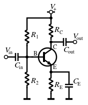
Amplifier circuit, common-emitter configuration with a voltage-divider bias circuit.
The common-emitter amplifier is designed so that a small change in voltage (Vin) changes the small current through the base of the transistor; the transistor's current amplification combined with the properties of the circuit mean that small swings in Vin produce large changes in Vout.
Various configurations of single transistor amplifier are possible, with some providing current gain, some voltage gain, and some both.
From mobile phones to televisions, vast numbers of products include amplifiers for sound reproduction, radio transmission, and signal processing. The first discrete-transistor audio amplifiers barely supplied a few hundred milliwatts, but power and audio fidelity gradually increased as better transistors became available and amplifier architecture evolved.
Modern transistor audio amplifiers of up to a few hundred watts are common and relatively inexpensive.
Comparison with vacuum tubes
Prior to the development of transistors, vacuum (electron) tubes (or in the UK "thermionic valves" or just "valves") were the main active components in electronic equipment.
Advantages
The key advantages that have allowed transistors to replace vacuum tubes in most applications are
- no cathode heater (which produces the characteristic orange glow of tubes), reducing power consumption, eliminating delay as tube heaters warm up, and immune from cathode poisoning and depletion;
- very small size and weight, reducing equipment size;
- large numbers of extremely small transistors can be manufactured as a single integrated circuit;
- low operating voltages compatible with batteries of only a few cells;
- circuits with greater energy efficiency are usually possible. For low-power applications (e.g., voltage amplification) in particular, energy consumption can be very much less than for tubes;
- inherent reliability and very long life; tubes always degrade and fail over time. Some transistorized devices have been in service for more than 50 years;
- complementary devices available, providing design flexibility including complementary-symmetry circuits, not possible with vacuum tubes;
- very low sensitivity to mechanical shock and vibration, providing physical ruggedness and virtually eliminating shock-induced spurious signals (e.g., microphonics in audio applications);
- not susceptible to breakage of a glass envelope, leakage, outgassing, and other physical damage.
Limitations
Transistors have the following limitations:
- silicon transistors can age and fail;
- high-power, high-frequency operation, such as that used in over-the-air television broadcasting, is better achieved in vacuum tubes due to improved electron mobility in a vacuum;
- solid-state devices are susceptible to damage from very brief electrical and thermal events, including electrostatic discharge in handling; vacuum tubes are electrically much more rugged;
- sensitivity to radiation and cosmic rays (special radiation-hardened chips are used for spacecraft devices);
- vacuum tubes in audio applications create significant lower-harmonic distortion, the so-called tube sound, which some people prefer.
Types
Transistors are categorized by
- semiconductor material (date first used): the metalloids germanium (1947) and silicon (1954)—in amorphous, polycrystalline and monocrystalline form—, the compounds gallium arsenide (1966) and silicon carbide (1997), the alloy silicon-germanium (1989), the allotrope of carbon graphene (research ongoing since 2004), etc. (see Semiconductor material);
- structure: BJT, JFET, IGFET (MOSFET), insulated-gate bipolar transistor, "other types";
- electrical polarity (positive and negative): n–p–n, p–n–p (BJTs), n-channel, p-channel (FETs);
- maximum power rating: low, medium, high;
- maximum operating frequency: low, medium, high, radio (RF), microwave frequency (the maximum effective frequency of a transistor in a common-emitter or common-source circuit is denoted by the term fT, an abbreviation for transition frequency—the frequency of transition is the frequency at which the transistor yields unity voltage gain)
- application: switch, general purpose, audio, high voltage, super-beta, matched pair;
- physical packaging: through-hole metal, through-hole plastic, surface mount, ball grid array, power modules (see Packaging);
- amplification factor hFE, βF (transistor beta) or gm (transconductance).
Hence, a particular transistor may be described as silicon, surface-mount, BJT, n–p–n, low-power, high-frequency switch.
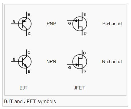
Bipolar junction transistor (BJT)
Bipolar transistors are so named because they conduct by using both majority and minority carriers. The bipolar junction transistor, the first type of transistor to be mass-produced, is a combination of two junction diodes, and is formed of either a thin layer of p-type semiconductor sandwiched between two n-type semiconductors (an n–p–n transistor), or a thin layer of n-type semiconductor sandwiched between two p-type semiconductors (a p–n–p transistor). This construction produces two p–n junctions: a base–emitter junction and a base–collector junction, separated by a thin region of semiconductor known as the base region (two junction diodes wired together without sharing an intervening semiconducting region will not make a transistor).
BJTs have three terminals, corresponding to the three layers of semiconductor—an emitter, a base, and a collector. They are useful in amplifiers because the currents at the emitter and collector are controllable by a relatively small base current. In an n–p–n transistor operating in the active region, the emitter–base junction is forward biased (electrons and holes recombine at the junction), and electrons are injected into the base region. Because the base is narrow, most of these electrons will diffuse into the reverse-biased (electrons and holes are formed at, and move away from the junction) base–collector junction and be swept into the collector; perhaps one-hundredth of the electrons will recombine in the base, which is the dominant mechanism in the base current. By controlling the number of electrons that can leave the base, the number of electrons entering the collector can be controlled. Collector current is approximately β (common-emitter current gain) times the base current. It is typically greater than 100 for small-signal transistors but can be smaller in transistors designed for high-power applications.
Unlike the field-effect transistor (see below), the BJT is a low-input-impedance device. Also, as the base–emitter voltage (VBE) is increased the base–emitter current and hence the collector–emitter current (ICE) increase exponentially according to the Shockley diode model and the Ebers-Moll model. Because of this exponential relationship, the BJT has a higher transconductance than the FET.
Bipolar transistors can be made to conduct by exposure to light, because absorption of photons in the base region generates a photocurrent that acts as a base current; the collector current is approximately β times the photocurrent. Devices designed for this purpose have a transparent window in the package and are called phototransistors.
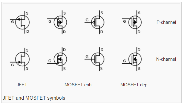
Field-effect transistor (FET)
The field-effect transistor, sometimes called a unipolar transistor, uses either electrons (in n-channel FET) or holes (in p-channel FET) for conduction. The four terminals of the FET are named source, gate, drain, and body (substrate). On most FETs, the body is connected to the source inside the package, and this will be assumed for the following description.
In a FET, the drain-to-source current flows via a conducting channel that connects the source region to the drain region. The conductivity is varied by the electric field that is produced when a voltage is applied between the gate and source terminals; hence the current flowing between the drain and source is controlled by the voltage applied between the gate and source. As the gate–source voltage (VGS) is increased, the drain–source current (IDS) increases exponentially for VGS below threshold, and then at a roughly quadratic rate (IGS ∝ (VGS − VT)2) (where VT is the threshold voltage at which drain current begins) in the "space-charge-limited" region above threshold. A quadratic behavior is not observed in modern devices, for example, at the 65 nm technology node.
For low noise at narrow bandwidth the higher input resistance of the FET is advantageous.
FETs are divided into two families: junction FET (JFET) and insulated gate FET (IGFET). The IGFET is more commonly known as a metal–oxide–semiconductor FET (MOSFET), reflecting its original construction from layers of metal (the gate), oxide (the insulation), and semiconductor. Unlike IGFETs, the JFET gate forms a p–n diode with the channel which lies between the source and drain. Functionally, this makes the n-channel JFET the solid-state equivalent of the vacuum tube triode which, similarly, forms a diode between its grid and cathode. Also, both devices operate in the depletion mode, they both have a high input impedance, and they both conduct current under the control of an input voltage.
Metal–semiconductor FETs (MESFETs) are JFETs in which the reverse biased p–n junction is replaced by a metal–semiconductor junction. These, and the HEMTs (high-electron-mobility transistors, or HFETs), in which a two-dimensional electron gas with very high carrier mobility is used for charge transport, are especially suitable for use at very high frequencies (microwave frequencies; several GHz).
FETs are further divided into depletion-mode and enhancement-mode types, depending on whether the channel is turned on or off with zero gate-to-source voltage. For enhancement mode, the channel is off at zero bias, and a gate potential can "enhance" the conduction. For the depletion mode, the channel is on at zero bias, and a gate potential (of the opposite polarity) can "deplete" the channel, reducing conduction. For either mode, a more positive gate voltage corresponds to a higher current for n-channel devices and a lower current for p-channel devices. Nearly all JFETs are depletion-mode because the diode junctions would forward bias and conduct if they were enhancement-mode devices; most IGFETs are enhancement-mode types.
Usage of bipolar and field-effect transistors
The bipolar junction transistor (BJT) was the most commonly used transistor in the 1960s and 70s. Even after MOSFETs became widely available, the BJT remained the transistor of choice for many analog circuits such as amplifiers because of their greater linearity and ease of manufacture. In integrated circuits, the desirable properties of MOSFETs allowed them to capture nearly all market share for digital circuits. Discrete MOSFETs can be applied in transistor applications, including analog circuits, voltage regulators, amplifiers, power transmitters and motor drivers.
Other transistor types

Transistor symbol created on Portuguese pavement in the University of Aveiro. With kind permission of Joao.pimentel.ferreira
Bipolar junction transistor (BJT):
- heterojunction bipolar transistor, up to several hundred GHz, common in modern ultrafast and RF circuits;
- Schottky transistor;
- avalanche transistor:
- Darlington transistors are two BJTs connected together to provide a high current gain equal to the product of the current gains of the two transistors;
- insulated-gate bipolar transistors (IGBTs) use a medium-power IGFET, similarly connected to a power BJT, to give a high input impedance. Power diodes are often connected between certain terminals depending on specific use. IGBTs are particularly suitable for heavy-duty industrial applications. The Asea Brown Boveri (ABB) 5SNA2400E170100 illustrates just how far power semiconductor technology has advanced. Intended for three-phase power supplies, this device houses three n–p–n IGBTs in a case measuring 38 by 140 by 190 mm and weighing 1.5 kg. Each IGBT is rated at 1,700 volts and can handle 2,400 amperes;
- phototransistor;
- multiple-emitter transistor, used in transistor–transistor logic and integrated current mirrors;
- multiple-base transistor, used to amplify very-low-level signals in noisy environments such as the pickup of a record player or radio front ends. Effectively, it is a very large number of transistors in parallel where, at the output, the signal is added constructively, but random noise is added only stochastically.
Field-effect transistor (FET):
- carbon nanotube field-effect transistor (CNFET), where the channel material is replaced by a carbon nanotube;
- junction gate field-effect transistor (JFET), where the gate is insulated by a reverse-biased p–n junction;
- metal–semiconductor field-effect transistor (MESFET), similar to JFET with a Schottky junction instead of a p–n junction;
- high-electron-mobility transistor (HEMT);
- metal–oxide–semiconductor field-effect transistor (MOSFET), where the gate is insulated by a shallow layer of insulator;
- inverted-T field-effect transistor (ITFET);
- fin field-effect transistor (FinFET), source/drain region shapes fins on the silicon surface;
- fast-reverse epitaxial diode field-effect transistor (FREDFET);
- thin-film transistor, in LCDs;
- organic field-effect transistor (OFET), in which the semiconductor is an organic compound;
- ballistic transistor;
- floating-gate transistor, for non-volatile storage;
- FETs used to sense environment;
- ion-sensitive field-effect transistor (IFSET), to measure ion concentrations in solution,
- electrolyte–oxide–semiconductor field-effect transistor (EOSFET), neurochip,
- deoxyribonucleic acid field-effect transistor (DNAFET).
- Tunnel field-effect transistor, where it switches by modulating quantum tunnelling through a barrier.
- Diffusion transistor, formed by diffusing dopants into semiconductor substrate; can be both BJT and FET.
- Unijunction transistor, can be used as simple pulse generators. It comprise a main body of either P-type or N-type semiconductor with ohmic contacts at each end (terminals Base1 and Base2). A junction with the opposite semiconductor type is formed at a point along the length of the body for the third terminal (Emitter).
- Single-electron transistors (SET), consist of a gate island between two tunneling junctions. The tunneling current is controlled by a voltage applied to the gate through a capacitor.
- Nanofluidic transistor, controls the movement of ions through sub-microscopic, water-filled channels.
- Multigate devices:
- tetrode transistor;
- pentode transistor;
- trigate transistor (prototype by Intel);
- dual-gate field-effect transistors have a single channel with two gates in cascode; a configuration optimized for high-frequency amplifiers, mixers, and oscillators.
- Junctionless nanowire transistor (JNT), uses a simple nanowire of silicon surrounded by an electrically isolated "wedding ring" that acts to gate the flow of electrons through the wire.
- Vacuum-channel transistor, when in 2012, NASA and the National Nanofab Center in South Korea were reported to have built a prototype vacuum-channel transistor in only 150 nanometers in size, can be manufactured cheaply using standard silicon semiconductor processing, can operate at high speeds even in hostile environments, and could consume just as much power as a standard transistor.
- Organic electrochemical transistor.
Part numbering standards/specifications
The types of some transistors can be parsed from the part number. There are three major semiconductor naming standards; in each the alphanumeric prefix provides clues to type of the device.
Japanese Industrial Standard (JIS)
JIS Transistor Prefix Table
|
Prefix |
Type of transistor |
|
2SA |
high-frequency p–n–p BJTs |
|
2SB |
audio-frequency p–n–p BJTs |
|
2SC |
high-frequency n–p–n BJTs |
|
2SD |
audio-frequency n–p–n BJTs |
|
2SJ |
P-channel FETs (both JFETs and MOSFETs) |
|
2SK |
N-channel FETs (both JFETs and MOSFETs) |
The JIS-C-7012 specification for transistor part numbers starts with "2S",[44] e.g. 2SD965, but sometimes the "2S" prefix is not marked on the package – a 2SD965 might only be marked "D965"; a 2SC1815 might be listed by a supplier as simply "C1815". This series sometimes has suffixes (such as "R", "O", "BL", standing for "red", "orange", "blue", etc.) to denote variants, such as tighter hFE (gain) groupings.
European Electronic Component Manufacturers Association (EECA)
The Pro Electron standard, the European Electronic Component Manufacturers Association part numbering scheme, begins with two letters: the first gives the semiconductor type (A for germanium, B for silicon, and C for materials like GaAs); the second letter denotes the intended use (A for diode, C for general-purpose transistor, etc.). A 3-digit sequence number (or one letter then 2 digits, for industrial types) follows. With early devices this indicated the case type. Suffixes may be used, with a letter (e.g. "C" often means high hFE, such as in: BC549C) or other codes may follow to show gain (e.g. BC327-25) or voltage rating (e.g. BUK854-800A). The more common prefixes are:
Pro Electron / EECA Transistor Prefix Table
|
Prefix class |
Type and usage |
Example |
Equivalent |
|
AC |
Germanium small-signal AF transistor |
AC126 |
NTE102A |
|
AD |
Germanium AF power transistor |
AD133 |
NTE179 |
|
AF |
Germanium small-signal RF transistor |
AF117 |
NTE160 |
|
AL |
Germanium RF power transistor |
ALZ10 |
NTE100 |
|
AS |
Germanium switching transistor |
ASY28 |
NTE101 |
|
AU |
Germanium power switching transistor |
AU103 |
NTE127 |
|
BC |
Silicon, small-signal transistor ("general purpose") |
BC548 |
2N3904 |
|
BD |
Silicon, power transistor |
BD139 |
NTE375 |
|
BF |
Silicon, RF (high frequency) BJT or FET |
BF245 |
NTE133 |
|
BS |
Silicon, switching transistor (BJT or MOSFET) |
BS170 |
2N7000 |
|
BL |
Silicon, high frequency, high power (for transmitters) |
BLW60 |
NTE325 |
|
BU |
Silicon, high voltage (for CRT horizontal deflection circuits) |
BU2520A |
NTE2354 |
|
CF |
Gallium Arsenide small-signal Microwave transistor (MESFET) |
CF739 |
— |
|
CL |
Gallium Arsenide Microwave power transistor (FET) |
CLY10 |
— |
Joint Electron Devices Engineering Council (JEDEC)
The JEDEC EIA370 transistor device numbers usually start with "2N", indicating a three-terminal device (dual-gate field-effect transistors are four-terminal devices, so begin with 3N), then a 2, 3 or 4-digit sequential number with no significance as to device properties (although early devices with low numbers tend to be germanium). For example, 2N3055 is a silicon n–p–n power transistor, 2N1301 is a p–n–p germanium switching transistor. A letter suffix (such as "A") is sometimes used to indicate a newer variant, but rarely gain groupings.
Proprietary
Manufacturers of devices may have their own proprietary numbering system, for example CK722. Since devices are second-sourced, a manufacturer's prefix (like "MPF" in MPF102, which originally would denote a Motorola FET) now is an unreliable indicator of who made the device. Some proprietary naming schemes adopt parts of other naming schemes, for example a PN2222A is a (possibly Fairchild Semiconductor) 2N2222A in a plastic case (but a PN108 is a plastic version of a BC108, not a 2N108, while the PN100 is unrelated to other xx100 devices).
Military part numbers sometimes are assigned their own codes, such as the British Military CV Naming System.
Manufacturers buying large numbers of similar parts may have them supplied with "house numbers", identifying a particular purchasing specification and not necessarily a device with a standardized registered number. For example, an HP part 1854,0053 is a (JEDEC) 2N2218 transistor which is also assigned the CV number: CV7763
Naming problems
With so many independent naming schemes, and the abbreviation of part numbers when printed on the devices, ambiguity sometimes occurs. For example, two different devices may be marked "J176" (one the J176 low-power JFET, the other the higher-powered MOSFET 2SJ176).
As older "through-hole" transistors are given surface-mount packaged counterparts, they tend to be assigned many different part numbers because manufacturers have their own systems to cope with the variety in pinout arrangements and options for dual or matched n–p–n+p–n–p devices in one pack. So even when the original device (such as a 2N3904) may have been assigned by a standards authority, and well known by engineers over the years, the new versions are far from standardized in their naming.
Construction
Semiconductor material
Semiconductor material characteristics
|
Semiconductor |
Junction forward |
Electron mobility |
Hole mobility |
Max. |
|
Ge |
0.27 |
0.39 |
0.19 |
70 to 100 |
|
Si |
0.71 |
0.14 |
0.05 |
150 to 200 |
|
GaAs |
1.03 |
0.85 |
0.05 |
150 to 200 |
|
Al-Si junction |
0.3 |
— |
— |
150 to 200 |
The first BJTs were made from germanium (Ge). Silicon (Si) types currently predominate but certain advanced microwave and high-performance versions now employ the compound semiconductor material gallium arsenide (GaAs) and the semiconductor alloy silicon germanium (SiGe). Single element semiconductor material (Ge and Si) is described as elemental.
Rough parameters for the most common semiconductor materials used to make transistors are given in the table to the right; these parameters will vary with increase in temperature, electric field, impurity level, strain, and sundry other factors.
The junction forward voltage is the voltage applied to the emitter–base junction of a BJT in order to make the base conduct a specified current. The current increases exponentially as the junction forward voltage is increased. The values given in the table are typical for a current of 1 mA (the same values apply to semiconductor diodes). The lower the junction forward voltage the better, as this means that less power is required to "drive" the transistor. The junction forward voltage for a given current decreases with increase in temperature. For a typical silicon junction the change is −2.1 mV/°C. In some circuits special compensating elements (sensistors) must be used to compensate for such changes.
The density of mobile carriers in the channel of a MOSFET is a function of the electric field forming the channel and of various other phenomena such as the impurity level in the channel. Some impurities, called dopants, are introduced deliberately in making a MOSFET, to control the MOSFET electrical behavior.
The electron mobility and hole mobility columns show the average speed that electrons and holes diffuse through the semiconductor material with an electric field of 1 volt per meter applied across the material. In general, the higher the electron mobility the faster the transistor can operate. The table indicates that Ge is a better material than Si in this respect. However, Ge has four major shortcomings compared to silicon and gallium arsenide:
- Its maximum temperature is limited;
- it has relatively high leakage current;
- it cannot withstand high voltages;
- it is less suitable for fabricating integrated circuits.
Because the electron mobility is higher than the hole mobility for all semiconductor materials, a given bipolar n–p–n transistor tends to be swifter than an equivalent p–n–p transistor. GaAs has the highest electron mobility of the three semiconductors. It is for this reason that GaAs is used in high-frequency applications. A relatively recent FET development, the high-electron-mobility transistor (HEMT), has a heterostructure (junction between different semiconductor materials) of aluminium gallium arsenide (AlGaAs)-gallium arsenide (GaAs) which has twice the electron mobility of a GaAs-metal barrier junction. Because of their high speed and low noise, HEMTs are used in satellite receivers working at frequencies around 12 GHz. HEMTs based on gallium nitride and aluminium gallium nitride (AlGaN/GaN HEMTs) provide a still higher electron mobility and are being developed for various applications.
Max. junction temperature values represent a cross section taken from various manufacturers' data sheets. This temperature should not be exceeded or the transistor may be damaged.
Al–Si junction refers to the high-speed (aluminum–silicon) metal–semiconductor barrier diode, commonly known as a Schottky diode. This is included in the table because some silicon power IGFETs have a parasitic reverse Schottky diode formed between the source and drain as part of the fabrication process. This diode can be a nuisance, but sometimes it is used in the circuit.
Packaging
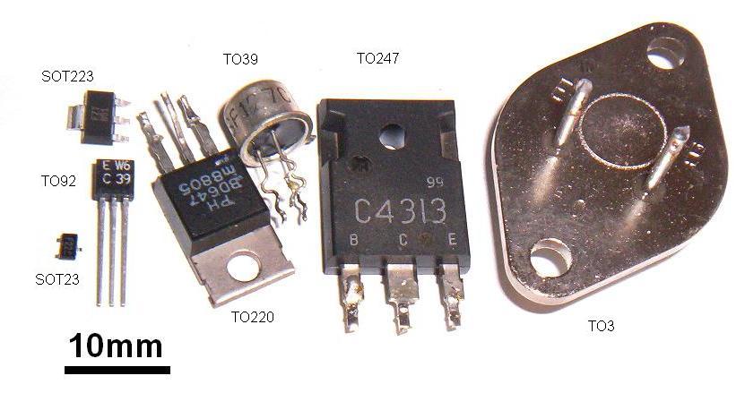
Assorted discrete transistors. With kind permission of Ulfbastel
Discrete transistors are individually packaged transistors. Transistors come in many different semiconductor packages (see image). The two main categories are through-hole (or leaded), and surface-mount, also known as surface-mount device (SMD). The ball grid array (BGA) is the latest surface-mount package (currently only for large integrated circuits). It has solder "balls" on the underside in place of leads. Because they are smaller and have shorter interconnections, SMDs have better high-frequency characteristics but lower power rating.
Transistor packages are made of glass, metal, ceramic, or plastic. The package often dictates the power rating and frequency characteristics. Power transistors have larger packages that can be clamped to heat sinks for enhanced cooling. Additionally, most power transistors have the collector or drain physically connected to the metal enclosure. At the other extreme, some surface-mount microwave transistors are as small as grains of sand.
Often a given transistor type is available in several packages. Transistor packages are mainly standardized, but the assignment of a transistor's functions to the terminals is not: other transistor types can assign other functions to the package's terminals. Even for the same transistor type the terminal assignment can vary (normally indicated by a suffix letter to the part number, q.e. BC212L and BC212K).
Nowadays most transistors come in a wide range of SMT packages, in comparison the list of available through-hole packages is relatively small, here is a short list of the most common through-hole transistors packages in alphabetical order: ATV, E-line, MRT, HRT, SC-43, SC-72, TO-3, TO-18, TO-39, TO-92, TO-126, TO220, TO247, TO251, TO262, ZTX851
Flexible transistors. Researchers have made several kinds of flexible transistors, including organic field-effect transistors. Flexible transistors are useful in some kinds of flexible displays and other flexible electronics.
Source: www.wikipedia.com